Solved consider the following circuit diagram which consists Cmos switching nmos vlsi transistor vss [overview] cmos inverter: definition, principle, advantages
Solved (a). Draw the schematic diagram of the CMOS | Chegg.com
Vlsi concepts: november 2014 3 input and gate circuit diagram Solved draw the cmos schematic for the given cmos layout
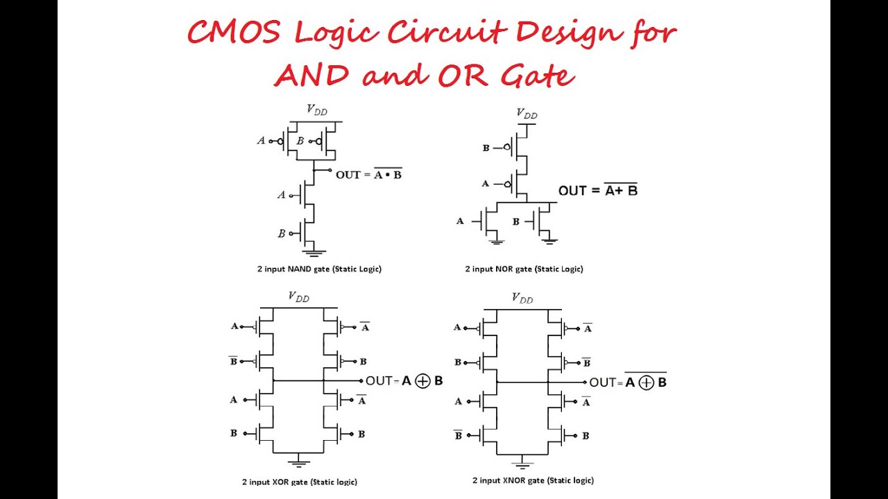
Design a input xor gate using cmos copeland trince
Cmos camera schematic diagramSolved (a) draw the schematic diagram for a standard cmos Cmos logic gates circuit diagramCmos xor gate schematic.
Solved: what is the cmos schematic? 1. draw the schematic. 2. identifyCmos input schematic vlsi 39e Cmos layout design rulesSolved (2) draw the schematic diagram for a standard cmos.

2 input nand gate cmos schematics pdf
Solved: chapter 9 problem 39e solutionWhat is cmos technology? Electronic – simplifying cmos schematic to reduce number of transistorsXor cmos logic transistor vsd exor mosfet inverter variable teltec fig2 circuits schematics.
Cmos circuitCmos circuit for example 2 Switching activity of cmosCmos schematic diagram.

Nand gate transistor diagram
Schematic diagram of a cmos inverter.Cmos-inverter| digital-cmos-design || electronics tutorial Cmos logic gates explainedCmos xor gate circuit diagram.
Cmos inverter circuit download scientific diagramCmos inverter 2 input and gate circuit diagram[diagram] stick diagram cmos inverter.
Electronic – minimum number of complementary cmos to implement \$f=abc+
Cmos inverterSchematic of a cmos inverter circuit Cmos layout design: introduction |vlsi conceptsCmos layout vlsi metal contact pmos connect diffusion introduction draw step contacts m1 which.
Cmos inverter circuit diagram principle minitool mosfet operation drain advantages definition general review resistors doesn makes contain any which gateCmos logic layout simple gates integrated circuits digital inverter ppt powerpoint presentation gnd dd Cmos inverter electronics tutorial digital figCmos inverter schematic.
![[Overview] CMOS Inverter: Definition, Principle, Advantages - MiniTool](https://i2.wp.com/www.minitool.com/images/uploads/lib/2021/01/cmos-inverter/cmos-inverter-1.png)
Solved (a). draw the schematic diagram of the cmos
Circuit diagram of cmos and gate .
.


Schematic diagram of a CMOS inverter. | Download Scientific Diagram

Circuit Diagram Of Cmos And Gate - Circuit Diagram

CMOS XOR gate circuit diagram | Download Scientific Diagram
2 Input And Gate Circuit Diagram

Nand Gate Transistor Diagram

PPT - CMOS Digital Integrated Circuits PowerPoint Presentation, free

Electronic – Minimum number of complementary CMOS to implement \$F=ABC+
